


Research
Combining radiation sensor and intelligent LSI circuit on a monolithic chip has been long desired in many field such as nuclear, high-energy physics, astrophysics, medical imaging, and material science. Such detector needs two kinds of Silicon (Si) crystals; one is thick high-purity Si layer for detecting radiation with high efficiency and the other is thin Si layer with many dopant for implementing high performance devices.
Present radiation imaging devices are mainly built from two different chips, one is sensor and the other is readout electronics, and these two are bonded with bulky metal bumps. Thus there are many unwanted materials which cause multiple scattering and the pixel size is limited by the bump size. Additionally, the readout speed and signal-to-noise ratio are limited with high spurious capacitances.
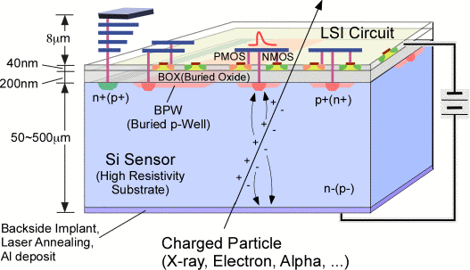
To improve the imaging device quality, we took use of the Silicon-On-Insulator (SOI) technology. We are using bonded SOI wafers of low resistivity Si on top for readout electronics, and high-resistivity Si (called handle wafer or substrate) at bottom for sensor. The two Si wafers are bonded via thin SiO2 (called BOX). Implantation of p+/n+ to the substrate is done after making halls in the top Si and BOX. Then contacts are formed to connect sensor with readout electronics of SOI layer. Above figure illustrates a basic structure of the SOI radiation image sensor.
This has a lot of advantages. There is no mechanical bump bonding, and thus less multiple scattering contributions. The pixel size can be much smaller compared with that of the imaging device with metal bump bonding. SOI processes are generally tolerant to radiation. Transistors formed on the SOI wafer have less parasitic capacitance compared with conventional bulk CMOS processes, helping circuit speed to be higher and power consumption to be lower.
R&D of radiation imaging sensors started in 2005 at KEK in collaborating with Lapis (former OKI) Semiconductor Co Ltd. which has technology of Fully-Depleted (FD) CMOS SOI process. Masks for the process were shared with other users (MPW : Multi Project Wafer) to reduce costs. The MPW runs KEK organized have been performed two times by 2008, and submissions are coming from researchers in US, Europe and China.
The smallest size of pixel designed so far is 8 x 8 um2. It will be used for beam monitors in high-energy experiment and X-ray application for material science which requires fast readout system. Another type of imaging sensors, counting or digital type, are also being developed. They will be used for X-ray imaging requiring high-rate and high-dynamic range applications and for high-energy charged particle trackers under severe radiation circumstances.
We are also doing many kinds of R&Ds which are nested implantations to handle wafer, 3D integration technique, Stitching for large area sensor, double SOI wafer, etc.
SOI Pixel Multi Project Wafer (MPW) run
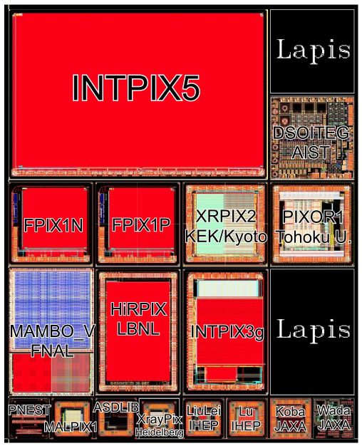
An example of MPW run mask.
Coming SOI MPW run Schedule:
We, KEK, are operating Multi Project Wafer (MPW) run of 0.2 um Silicon-On-Insulator (SOI) pixel process periodically (1~2 runs / year) This MPW run is open to all over the world. If you would like to join the MPW run, please send email to Yasuo Arai (yasuo.arai@kek.jp) .
Brief summary of the SOI process
Process : Lapis Semiconductot Co. Ltd. Fully-Depleted 0.2um SOI CMOS Pixel process.
Wires : 1 Poly + 5 metal layers.(minimum wire pitch is 0.58um)
Voltage : 1.8 V for core transistors, 3.3 V for I/O transistors.
Transistors : Low threshold, High threshold, I/O, and DMOS
Body-Floating, Body-Tie, Source-Tie (2 kinds).
Wafers : CZ(n ~700ohm-cm)/FZ(n ~2 kohm-cm)/FZ(p ~25kohm-cm) (Wafer types might be changed depend on the availability)
[Special Features]
Creation of sensor diodes in handle wafer (p+ and n+ implantation).
MIM capacitor (1.5 fF/um2, Minimum MIM capacitance size is 5um x 5um), poly resistor, lateral diode
.
Buried p-well (p implant to handle wafer through surface Si)
Buried n-well (n implant to handle wafer through surface Si)
176 pins & 220 pins ceramic PGA package are available.
[Advanced Options]
Double SOI wafer process
3D vertical integration option with T-micro u-bump technology (5um pitch)
[CAD environment]
Cadence Virtuoso layout editor with parameterized cell.
HSPICE simulation model
Mentor Calibre Design Rule check
Star-RCXT or Mentor Calibre RC Extraction
Links
Last modified Aug. 29, 2019